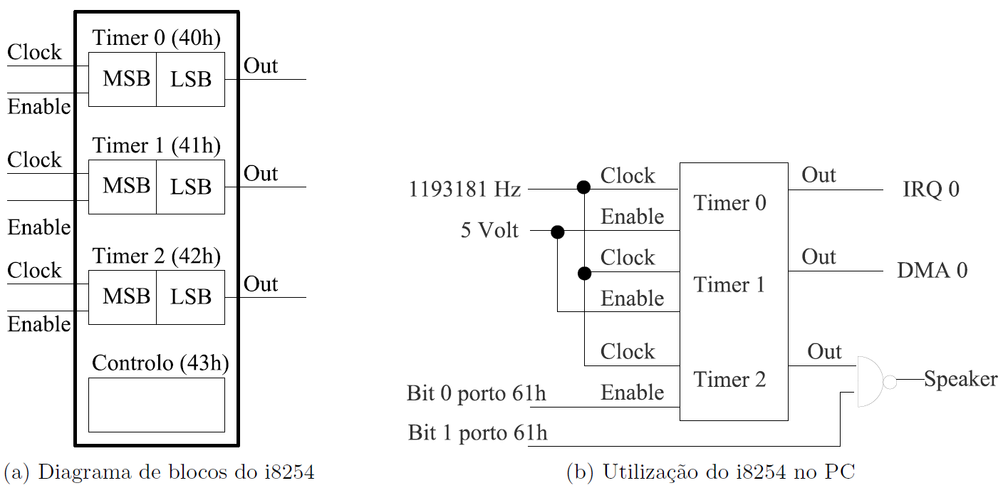
Figure 1: The PC's timer: i8254.
Every PC "has" an i8254 an integrated circuit (IC) with 3 timers, whose block diagram is shown in Figure 1. In this lab, you'll use timer 0 only. You must not change timer 1 configuration.
The 3 timers are identical and operate independently of one another. Thus we will describe only one timer.
A timer has a 16 bit counter, two input lines, Clock and Enable, and an output line Out. The Enable line is used to enable/disable the timer. When a timer is enabled, the value of its counter is decremented by one on every pulse of the Clock line. The value of Out depends on the counter's value and on the operating mode.
The i8254 supports several modes, but in this lab you will use only mode 3, square wave generator, because this is the mode Minix configures all timers. In this mode, the Out line is high initially and until the counter reaches half of its initial value. It then goes low until the counter reaches zero, at which time the counter is reloaded with its (pre-programmed) initial value, Out is set to high and the cycle begins again. Thus, in mode 3, the timer generates a square wave with a frequency given by the expression clock/div, where clock is the frequency of the Clock input and div is the value loaded initially in the timer.
Each timer has a 16 bit counter, which may be both read and written. Furthermore, the i8254 has a single control register that can be written only, and that is used to configure the operation of all timers.
Each timer is programmed independently of the other timers. Programming a timer requires two steps:
The format of the control word (a 8-bit value) is shown in Table 1.
| Bit | Value | Function |
| Select counter | ||
| 7,6 | 00 | 0 |
| 01 | 1 | |
| 10 | 2 | |
| Type of Access | ||
| 5,4 | 01 | LSB |
| 10 | MSB | |
| 11 | LSB followed by MSB | |
| Operating Mode | ||
| 3,2,1 | 000 | 0 |
| 001 | 1 | |
| 010 | 2 | |
| 110* | ||
| 011 | 3 | |
| 111* | ||
| 100 | 4 | |
| 101 | 5 | |
| Counting mode | ||
| 0 | 0 | Binary (16 bits) |
| 1 | BCD (4 decades) |
Thus, bits 6 and 7 specify which timer to program. Bits 1, 2 and 3 specify the operating mode. Bit 0 specifies whether the counter is a binary or a BCD counter, i.e. whether the inital value should be interpreted as a binary or a BCD value. Bits 4 and 5 specify how the initial value is loaded. The following paragraph provides some more details regarding these bits.
Although the counters are 16 bits, the i8254 has only 8 data lines. Thus to load the initial value of a counter, the LSB and the MSB must be written separately. The i8254 allows loading either of these bytes, or both of them. In the latter case, the LSB must be loaded first. Which bytes of the counter will be loaded in the second step of the programming procedure of a timer is specified by bits 4 and 5.
Reading a timer's configuration requires a special command: the Read-Back command. This command allows not only to read the programmed mode, but also the count value and the current state of the OUT line of the selected timer(s). Table 2 shows the format of the Read-Back command.
| Bit | Value | Function |
| 7,6 | 11 | Read-Back Command |
| 5 | COUNT | |
| 0 | Read counter value | |
| 4 | STATUS | |
| 0 | Read Programmed Mode | |
| 3 | Select Counter 2 | |
| 1 | Yes | |
| 2 | Select Counter 1 | |
| 1 | Yes | |
| 1 | Select Counter 0 | |
| 1 | Yes | |
| 0 | 0 | Reserved |
Like the Control word, the Read-Back command is also written to the control register. The value of bits 6 and 7, allow the i8254 distinguish between a control word and a read-back command.
Selection of the counters is now done with the help of a bit mask -- bits 1 to 3 --, thus allowing to retrieve information regarding different timers with a single command.
Likewise selection of the data to read uses a bit mask -- bits 4 and 5,-- thus allowing to read either the count value or the programmed mode, or both. Note that these bits are active low, i.e. the associated action occurs only when their value is 0, not 1, hence the bar over their names.
In this lab, you need to read the configuration of only one timer at a time. Thus after writing the appropriate Read-Back command to the control register, the configuration can be obtained by reading from that timer. You can find further details on the operation of the Read-Back command on the corresponding Section on pg. 7 of the i8254 data sheet.
Table 3 shows the format of a timer's Status byte:
| Bit | Function |
| 7 | Output |
| 6 | Null Count |
| 5, 4 | Type of Access |
| 3,2,1 | Programmed Mode |
| 0 | BCD |
That is, bits 0 to 5 contain the corresponding bits of the last control word affecting the operation of that timer.
Bit 7 contains the current value of the timer's OUT line. Finally, bit 6 is related to the reading of the counting value, and we do not provide further details. You can find them in the i8254 data sheet.
The PC uses each timer for a different purpose. Nevertheless, all timers use the same clock signal with frequency 1193181 Hz.
As shown in Figure 1, the output of timer 2 is connected to the PC speaker, and is used to generate tones by generating a square wave of an audible frequency. For example, to generate a 1000 Hz tone, the timer must be programmed to operate in mode 3, with an initial value of 1193.
Furthermore, to enable the speaker, you must set to 1 both bits 0 and 1 of I/O port 0x61 (SPEAKER_CTRL) . As shown in Figure 1, bit 0 is connected to the GATE of Timer 2 and if low, it will disable the timer. In addition, the OUT line of timer 2 is not connected directly to the speaker, instead it is gated via a NAND, whose other input line comes from bit 1 of port 0x61. Thus, unless that bit is set to 1, the input to the speaker will always be high, and no tone will be generated.
Note: On most laptops VBox does not emulate the speaker. Therefore, you will not be able to hear any tone, even if you correctly configure the Timer 2.
Figure 1 also shows that the output of the timer 0 is directly connected to line IRQ0 of the PC's interrupt controller. It is usually programmed in mode 2, to generate a more or less stable time reference that can be used by the operating system to measure time with a resolution of a few milliseconds. In Section 4 we describe the interrupt mechanism used by the PC, and in Section 5 we describe the use in Minix 3 of the interrupts generated by the timer 0.
The registers of the i8254, like those of most other PC's I/O devices, are mapped in the I/O address space of the PC's processor. The address of the control register (TIMER_CTRL) is 0x43, the address of timer 0 is 0x40 (TIMER_0) and the address of timer 2 is 0x42 (TIMER_2). Although the counters of these timers are 16 bit, all these registers are 8 bits, and access to the MSB and the LSB of each counter is done as described above in Section 3.2.